Figure 19-7 illustrates another approach to digital-to-analog conversion. The operational amplifier is used to produce a weighted slim of the digital inputs, where the weights are proportional to the weights of the bit positions of the inputs. Recall from Chapter 13 that each input is amplified by a factor equal to the ratio of the feedback resistance divided by the input resistance to which it is connected. Thus, DJ. the most significant bit, is amplified by R,IR, D2 by R,/2R = 1I2(R,IR), DI by Rtl4R = 1I4(R,IR), and D” by R,/8R = 1I8(R,IR). Since the amplifier sums and .inverts, the output is


The principal disadvantage of this type of converter is that a different-valued precision resistor must be used for each digital input. In contrast, the R-2R ladder network uses only two values of resistance.
Example 19-2
Design a 4-bit, weighted-resistor DAC whose full-scale output voltage is -10 V. Logic levels are 1’= +5 V and 0 == 0 V. What.is the output voltage when the input is 101O?
Solution
The full-scale output voltage is the output voltage when the input is
maximum: 1111. In that case, from equation 19-2, V!c require
or
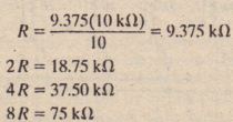
Let us choose R, = 10 kO. Then
When the input is 1010, the output voltage is
THE SWITCHED CURRENT·SOURCED DAC
The D/A converters we have discussed so far can be regarded as switched voltagesource’ converters: When a binary input goes high, the high voltage is effectively switched into the circuit, where it is summed with other input voltages. Because of the technology used to construct integrated-circuit DACs, currents can be switched in and out of a circuit faster than voltages can. For that reason, most integrated circuit DACs utilize some form of current switching, where the binary inputs are used to open and close switches that connect and disconnect internally generated currents. The currents are weighted according to the bit positions they represent and are summed in an operational amplifier. Figure 19-8 shows an example. Note that an R-2 R ladder is connected to a voltage source identified. as EKI!'” The current that tlows in each 2 R resistor is
The D/A converters we have discussed so far can be regarded as switched voltagesource’ converters: When a binary input goes high, the high voltage is effectively switched into the circuit, where it is summed with other input voltages. Because of the technology used to construct integrated-circuit DACs, currents can be switched in and out of a circuit faster than voltages can. For that reason, most integratedcircuit DACs utilize some form of current switching, where the binary inputs are used to open and close switches that connect and disconnect internally generated currents. The currents are weighted according to the bit positions they represent and are summed in an operational amplifier. Figure 19-8 shows an example. Note that an R-2 R ladder is connected to a voltage source identified. as EKI!'” The current that tlows in each 2 R resistor is
when 11 = I) N – I is the subscript for the current created by input D; and N is the total number of inputs. Thus, each current is weighted according to the bit position it represents. For example, the current in the 2 R resistor at the D, input in the figure (Il = 1 and N = 4) is (EREF /R)(1/2)3. The binary inputs control switches that connect the currents either to ground or to the input of the amplifier. The amplifier sums all currents whose corresponding binary inputs arc high. The amplifier also serves as a current-to-voltage converter. It is connected in an inverting . configuration and its output is
where Iris the sum of the currents that have been switched to its input. For example, if the input is 1001, then

and
Example 19-3
The switched current-source DAC in Figure 19-8 has R = 10 k!l and Ell.Ill=’ 10 Y. Find the total current delivered to the amplifier and the output voltage when the binary input is 1010.
Solution.
From equation (19-3)
and
The reference voltage EKEl’in.Pigure 19-H may be fixed-as, for example, when It is generated internally in an integrated circuit-or it may be externally variable. When it is externally variable, the output of the DAC is proportional to the product of the variable EREIa’ nd the variable binary input. In that case, the circuit is called a multiplying D/A converter, and the output represents the product of an analog input (EREI’)and a digital input
In most integrated-circuit DACs utilizing current-source switching, the output is the total current IT produced in the R-2 R ladder. The user may then connect a variety of operational amplifier configurations af the output to perform magnitude scaling and/or phase inversion. If EKEIc’an be both positive and negative and if the
binary input always represents a positive number, then the output of the DAC is both positive and negative. In that case, the DAC is called a two-quadrant multiplier. A DAC whose output can be both positive and negative is said to be bipolar, and one whose output is only positive or only negative is unipolar. A four-quadrant multiplier is one in which both inputs can be either negative or ~positive and in which the output (product) has the correct sign for every casco Negative binary inputs can be represented using the offset binary code, the 4-bit version of which is shown in Table 19-1. Note that the numbers +7 through -8 are represented by 0000 through 1111, respectively, with 0)10 represented by 1000.The table also shows the analog outputs that are produced by a multiplying D/A converter. In general, for an N-bit DAC, the offset binary code represents decimal numbers from +2N-1 – I through -2N-1 and the analog outputs range from


