ZENER DIODES
In.earlier chapters we discussed several zener-diode applications, perhaps the most important of which is the zener voltage reference used in regulator circuits. We wish now to examine the characteristics and limitations of these devices in more detail, so we can interpret and apply specifications for some of their important parameters.
Figure 18-1 shows a typical 1- V characteristic for a zener diode. The forward biased characteristic is identical to that of a forward-biased silicon diode and obeys the same diode equation that we developed in Chapter 2 (equation 2-13). The zener diode is normally operated in its reverse-biased breakdown region, where the voltage across the device remains substantially ‘Constant as the reverse current varies over a large range. Like a fixed voltage source, this ability to maintain a constant voltage across its terminals, independent of current, is what makes the device useful as a voltage reference. The fixed breakdown voltage is called the crated in the ‘figure


The Zener-Diode Voltage Regulator
To demonstrate how a zener diode can serve as a constant voltage reference, Figure lR-2 shows a simple but widely used configuration that maintains a constant voltage across a load resistor. The circuit is an elementary ooltag» regulator (see Section 17-7) th:lt holds the load voltage near V;: volts as R” and/or VII undergo changes. So the voltage across the parallel combination of the zener and Rio remain at Vz volts, the reverse current lz through the diode must at all times be large enough to keep the device in its breakdown region, as shown in Figure 18-1. The value selected for Rs is critical in that respect. As we shall presently demonstrate, Rs must be small enough to permit adequate zener current, yet large enough to prevent the zener current and power dissipation from exceeding permissible limits. It is apparent in Figure 18-2 that
Example 18-1
1. the minimum and maximum currents in the zener diode;
2. the minimum and maximum power dissipated in the diode; and
3. the minirru.,u rated power dissipation that Rs should have.
sotution
1. Assuming that the zener diode remains in breakdown, then till: load voltage remains constant at Vz = 18 V, and the load current therefore remains constant at
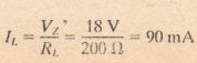
From equation 18-2, when V;” = 20 V,
![]()
2. PzCmin) = VzIz(min) = (18 V)(IO mA) = 180 mW
PAmax) = VzIzCmax) = (18 V)(510 mA) = 9.18 W
3. PRs(max) = l}(max)Rs = (0.6)2(20) = 7.2 W
The reverse current in a certain 10-V, 2-W zener diode must be at least 5 mA to ensure that the diode remains in breakdown. The diode is to be used ill the regulator circuit shown in Figure 18-3, where Vin can vary from 15 V to 20 V. Note that the load can be switched out of the regulator circuit in this application. Find a value for Rs. What power dissipation rating should Rs have?

Solution

Therefore, from inequality 18-7,

From inequality 18-8,
![]()
Temperature Effects
The breakdown voltage of a zener diode is a function of the width of its depletion region, which is controlled during manufacturing by the degree of impurity doping Recall that heavy doping increases conductivity, which narrows the depletion region, and therefore decreases the voltage at which breakdown occurs. Zener diodes are available with breakdown voltages ranging from 2.4 V to 200 V. As noted in Chapter 2, the mechanism by which breakdown occurs depends on the breakdown voltage itself. When Vz is less than about 5 V, the high electric field intensity across the narrow depletion region (around 3 X 10⁷ VIm) strips carriers directly from their bonds, a phenomenon usually called zener breakdown. For Vz greater than about 8 V, breakdown occurs as a result of collisions between high-energy carriers, the mechanism called avalanching. Between 5 V and 8 V, both the avalanching and zener mechanisms contribute to breakdown. The practical significance of these facts is that the breakdown mechanism determines how temperature variations affect the value of Vz. Low-voltage zener diodes that break down by the zener mechanism have negative temperature coefficients (Vz decreases with increasing temperature) and higher-voltage avalanche zeners have positive temperature coefficients. When Vz is between about 3 V and 8 V, the temperature coefficient is also strongly influenced by the current in the diode: the coefficient may be positive or negative, depending on current, becoming more positive as current increases. The temperature coefficient of a zener diode is defined to be its change in breakdown voltage per degree Celsius increase in temperature. For example, a temperature coefficient of +8 mV/oC means that Vz will increase 8 mV for each degree Celsius increase in temperature. Temperature stability is the ratio of the temperature coefficient to the breakdown voltage. Expressed as a percent,

where T.C. is the temperature coefficient. Clearly, small values of S are desirable. In applications requiring a zener diode to serve as a highly stable voltage reference, steps must be taken to temperature compensate the diode. A technique that is used frequently is to connect the zener in series with one or more semiconductor devices whose voltage drops change with temperature in the’ opposite way that Vz changes, i.e., devices having the opposite kind of temperature coefficient. If a temperature change causes Vz to increase, then the voltage across the other components decreases, so the total voltage across the series combination is (ide Ily) unchanged. For example, the temperature coefficient of a forward-biased silicon diode is negative, so une or more of these can be connected in series with a zener diode having a positive temperature coefficient, as illustrated in Figure 18-4. The next example illustrates that several forward-biased diodes, which have relatively small temperature coefficients, may be required to compensate a single zener diode.
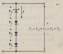
A zener diode having a breakdown voltage of 10 V at ,25~C has a temperature coefficient of +5.5 mVre. It is to be temperature compensated by connecting it in series with three forward-biased diodes, as shown in Figure 18-4. Each compensating diode has a forward drop of 0.65 V at 25°C and a temperature coefficient of -2 «vrc.
1. What is the temperature stability of the uncompensated zener diode?
2. What is the breakdown voltage of the uncompensated’zener diode at 100°C?
3. What is the voltage across the compensated network at 25°C? At 100°C?
4. What is the temperature stability of the compensated network
Solution
1. From equation 18-9
![]()
2. Vz = (10 V) + ~T(T.e.) = (10 V) + (100°C – 25°C)(5.5 mV/°C) = 10.4125 V
3. As shown in Figure 18-4, Vo = Vz + VI + V2 + V3• At 25°C, Vo = 10 +
3(0.65) = 11.95 V. At 100°C, the drop Vd across each forward-biased diode is
Vd = (0.65 V) + (100°C – 25°C)(-2 mV/°C) = 0.5 V. Therefore, at 100°C,
Vo = (10.4125 V) + 3(0.5 V) = 10.5625 V.
4. The temperature coefficient of the compensated network is T.e. = (+5.5 mV/ 0C) + 3( -2 mV/°C) = (+5.5 mV/°C) – (6 mV/°C) = -0.5 mvre. The voltage drop across the network (at 25°C) was found to be 11.95 V, so
![]()
We see that compensation has improved the stability by a factor gr.eater than 10.
Temperature-compensated zener diodes are available from manufacturers in single-package units called reference diodes. These units contain specially fabricated junctions that closely track and oppose variations in Vz with temperature. Although it is possible to obtain an extremely stable reference this way, it may be necessary to maintain the zener current at a manufacturer’s specified value in order to realize the specified stability. Figure 17-43 shows a temperature-stabilized zener diode whose current is maintained by a constant-current source to ensure its stability as reference for the 723 voltage regulator
Zener-Diode Impedance
The breakdown characteristic of an ideal zener diode is a perfectly vertical line, signifying zero change in voltage for any change in current. Thus, the ideal diode has zero impedance (or ac resistance) in its breakdown region. A practical zener diode has nonzero impedance, which can be computed in the usual way:
![]()
Zz is the reciprocal of the slope of the breakdown characteristic on an l r: Vz plot. The slope is not constant, so the value of Zz’ depends on the point along the characteristic where the measurement is made. The impedance decreases as lz increases; that is, the breakdown characteristic becomes steeper at points farther down the line, corresponding to greater reverse currents. For this reason, the diode should be operated with as much reverse current as possible, consistent with rating limitations. Manufacturers’ specifications for zener impedances are usually given for a specified 6./z that covers a range from a small Iz near the onset of breakdown to some percentage of the maximum rated /z. The values may range from a few ohms to several hundred ohms. There is also a variation in the impedance of zener diodes among those having different values of Vz. Diodes with breakdown voltages near 7 V have the smallest impedances.
Example 18-4
A zener diode has impedance 40 !l in the range from lz = 1 mA to Lz = 10 mA. The voltage at lz = 1 mA is 9.1 V. Assuming that the impedance is constant over the given range, what minimum and maximum zener voltages can be expected if the diode is used in an application where the zener current changes from 2 mA to 8mA?
Solution.
From equation’ 18-10, the voltage change between lz ~ 1 mA and lz = 2 mA is 6.Vz = MzZz = [(2 mA) – (1 mA)](40!l) = 0.04 V. Therefore, the minimum voltage is Vz(min) = (9.1 V) + 6.Vz = (9.1 V) + (0.04 V) = 9.14 V. The voltage change between lz = 2 mA and Lz = 8 mA is 6.Vz = [(8 mA) (2 mA)](40 !l) = 0.16 V. Therefore, the maximum voltage is VzCmax) Vz(min) + 6.Vz = (9.14 V) + (0.16 V) = 9.3 V.