Four-layer devices, also called thy ristors, comprise a class of semiconductor components whose structure is characterized by alternating layers of P and N material. By altering the terminal configuration anti geometry of the basic structure, it is possible to construct a variety of useful devices- including silicon controlled reotifiers, silicon controlled switches, diacstriacs, and Shockley diodes. These are. widely used in high-power switching applications where the control of hundreds of amperes and thousands of watts is not unusual. They are especially useful in the control of ac power delivered to heavy loads such as electric motors and lighting systems.
Silicon Controlled Rectifiers (SCAs)
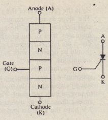
Figure 18-5 shows the layered PNPN structure of a silicon controlled rectifier (SCR). Note that there are three PN junctions in this structure. The figure also shows the schematic symbol for an SCR and its three terminals: anode (A), gate. (D), and cathode (K). In applications, the anode is made positive with respect to . the cathode. As the name and symbol imply, the SCR behaves like a diode (rectifier), which is normally forward biased, bUI conducts from anode to cathode only if a control signal is applied to the gate
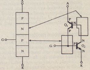
As an aid in understanding SCR operation, Figure 18-6 shows a two-transistor equivalent of the four-layer device. Note that the Nand P layers in the center of the structure arc “shared” by the transistors: the N layer is the base of 01 and the collector of O2, while the P layer is the collector of 01 and the base of O2,
In our analysis of SCR operation, we will first consider the case where the gate is open and a positive voltage VA is connected between anode and cathode. as shown in Figure 18-7. The positive voltage forward biases the emitter-base junction of 01′ However, the base current in QI is only a small leakage current because the base of QI” is the collector of Q2 and the collector-bas-e junction of 02 is reverse biased. The only base current in Q2 is a small leakage current from 0,. Thus. both the base and collector currents in Q2 are small leakage currents. Since the emitter current in Q2 is the same as the total current flowing through the SCR. and since 1/::2= 1m + lei, we see that the total SCR current is the sum of two small leakage currents. which we may regard as negligibly small. We say that the SCR itself is off (essentially nonconducting). or in a forward blocking state: forward biased. but blocking the flow of current
SCR operation is based on the fundamental principle that the a and f3 of a transistor remain small so long as its collector current is small. As we saw in Chapter4. collector current must be increased to a certain level before those parameters acquire the normal, essentially constant values they have in the active region. When

Once the SCR has switched on, it will remain on provided the current through it remains sufficiently large. If the current is reduced (by reducing VA, for example) to the point that fA falls below a certain holding current, then the SCR will revert to its off state. The holding current, Iu, is identified in Figure 18-9(b) as the flat portion of the characteristic corresponding to the regenerative switching region
Note that the SCR cannot remain in this region for any length of time; the horizontal line merely shows the path followed when the SCR switches on, and is often drawn as a dashed line for that reason
Shockley Diodes
In all our analysis to this point, we have assumed that the gate terminal is open, so lo remained 0 at all times. Certain four-layer devices are manufactured without gate terminals, so they behave exactly like an SCR with an open gate. These twoterminal devices are called Shockley diodes, or four-layer diodes. Figure 18-10 shows the schematic symbol for a Shockley diode and an application called a relaxation oscillator. Capacitor C charges through R to the breakover voltage, at which time the diode switches on and quickly discharges the capacitor. The diode then turns off and the capacitor begins charging again. The frequency of oscillation is controlled by the RC time constant.
SCR Triggering
SCRs are normally operated with an external circuit connected to the gate. The purpose of the circuit is to inject current into the base of Q2 in Figure 18-8 and thereby “trigger” the SCR into a regenerative breakover. The additional current supplied by the gate causes IC2 to increase, which increases let, and so forth, so the SCR switches to its on state, as before. Thus, the gate serves as a control input that can be used to switch the SCR from off to on when desired. It is important to realize that it is necessary to supply only a short pulse of current through the gate to cause the switching action; once the regeneration is initiated, latching quickly occurs and gate current is no longer required. By the same token, the SCR cannot be turned off by simply reducing gate current to O.As described earlier, it can be turned off only by reducing the anode-to-cathode current to a value below the holding current.
Figure 18-11 is a typical family of SCR characteristics showing IA versus \.:’AK .for different values of gate current. Notice that the larger the gate current, the . smaller the break over voltage. When gate current is large, it is flat necessary for
We will now derive a general expression for the SCR current 1″ in terms of gate current lc and leakage currents fCBOI and l cnoi- The result will demonstrate vividly how the magnitudes of al and a2affect the SCR current below and at the onset of breakover. In our derivation we will u .e the following two relations, which are easily obtained from the standard transistor equations given in Chapter 4 (4-4 and 4-9):
Equation 18-18 shows that if a, and a2 are small, the current fA is essentially the sum of two small leakage currents. However, if this current, pIus the component of gate current, increases enough to raise the values of a, and a2 to where a, + a2 = 1, the denominator of (18-18) becomes O. In that case fA is theoretically infinite, limited only by external resistance.
Half-Wave Power Control Using SeRs
SCRs are commonly used to adjust, or control, the average power delivered to a load from an ac source. In these applications, the SCR is periodically switched on and off, and the average power delivered to the load is controlled by adjusting the total length of time the SCR conducts during each ac cycle. Figure 18-14 shows a
simple half-wave power controller based on this principle.
When the ac voltage in Figure 18-14 is positive and the SCR is conducting, current flows through load resistance RI .. As shown in (b) and (c), the total length of time the SCR conducts depends on the point in each cycle at which the SCR switches on, or fires. After firing, the SCR continues to conduct until the ac voltage drops to near 0, causing the SCR current to fall below the holding current. It then remains off until firing again at the san;te point in the next positive half-cycle. The angle of the ac waveform at which the SCR switches on is called the firing angle, Or, or the delay angle. The firing angle is controlled by adjusting R, _When R, is large, the ac voltage must reach a large value to generate enough gate current to
fire the SCR. Consequently, the firing angle is large, as shown in Figure 18-14(c}. Conversely, when R, is small. a relatively small voltage will cause the SCR to fire, and Or will be small. In the circuit shown, Or can be adjusted from 0° to 90°_ The diode is used to protect the gate from the negative portion of the ac voltage.
One problem encountered in practical applications of SCRs, particularly high power devices. is a tendency to “false-trigger” if there is a large, nile of change of anode voltage. This tendency is attributable to the large junction capacitance associated with the large junction areas that are necessary to dissipate heavy amounts of power. Recall that capacitor current is proportional to the rate of change of capacitor voltage. The large charging current that results when the anode voltage changes at a high rate may induce regenerative brcnkovcr, To suppressa false triggering. a shunting capacitor is sometimes connected between anode and cathode.


