Cancellation of even Harmonics
Recall that push-pull operation effectively produces in a load a waveform proportional to the difference between two input signals. Under normal operation the signals are out of phase so their waveform is reproduced in the load. If the signals were in phase cancellation would occur. It is instructive to view a push-pull output as the difference between two distorted (half-wave rectified) sine waves that are out of phase with each other. This viewpoint is illustrated in Figure 16-21. It can be shown that a half-wave-rectified sine wave contains only the fundamental and ; II even harmonics. Figure 16-21(a) shows the two out-of-phase half-wave-rectified sine waves that drive the load. and 16-21 (b) shows the fundamental and second harmonic components of each. Notice that the fundamental components arc out of phase. Therefore, the fundamental component is reproduced in the load, as we have already seen (Figure 16-10). However the second-harmonic components are in .phase, and therefore cancel in the load. Although not. shown .in this figure, the fourth and all other even harmonics are also in phase and therefore also cancel.

Our conclusion is an important property of push-pull amplifiers: even harmonics are cancelled in push-pull operation
The cancellation of even harmonics is an important factor in reducing distortion in push-pull amplifiers. However, perfect cancellation would occur only if the two sides were perfectly matched and perfectly balanced: identical transistors, identical drivers, and a perfectly center-tapped transformer. Of course, this is not the case in practice, but even imperfect push-pull operation reduces even harmonic distortion. Odd harmonics are out of phase, so cancellation of those components does not occur
Crossover Distortion
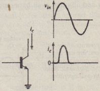
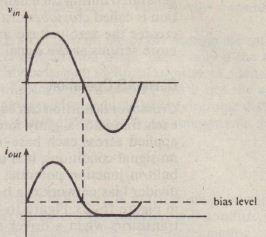
Recall that a forward-biasing voltage applied across a PN junction must be raised to a certain level (about 0.7 V for silicon) before the junction will conduct any significant current. Similarly the voltage across the base-emitter junction of a transistor must reach that level before any appreciable base current and hence current can flow. As a consequence, the drive signal applied to a class-B transistor must reach a certain minimum level before its collector current is properly in the active region. This fact is the principal source of distortion in a class-B, push-pull amplifier, as illustrated in Figure 16-22. Figure 16-22(a) shows that the initial rise of collector current in a class-B transistor lags the initia rise of input voltage for the reason we have described. Also collector current prematurely drops to 0 when the input voltage approaches O. Figure 16-22(b) shows the voltage waveform that is produced in the load of a push tmll amplifier when the distortion

(a> Collector current in a class-B transistor does not follow input voltage in the regions near 0 (crossovers>
(b) The load voltage in a class-B push-pull amplifier. showing the combined effects of generated during each half-cycle of input generated during each half-cycle by each class-B transistor is combined. This distortion is called crossover distortion because it occurs where the composite waveform crosses the zero-voltage axis. Clearly, the effect of crossover distortion becomes more serious as the signal level becomes smaller.
Class-AB Operation
Crossover distortion can be reduced or eliminated in a push-pull amplifier by biasing each transistor slightly into conduction. When a small forward-biasing voltage is applied across each base-emitter junction, and a small base current flows under no-signal conditions, it is not necessary for the base drive signal to overcome the built-in junction potential before active operation can occur. A simple voltage divider bias network can be connected across each base for this purpose, as shown in Figure 16-23. Figure 16-23(a) shows how two resistors can provide bias for both transistors when a driver transtormer is used. Figure 16-23(b) shows the use of two voltage dividers when the drive signals are capacitor-coupled. Typically the

Methods [or providing II slight forward bias for push-pull transistors 10 reduce crossover distortion

base-emitter junctions are biased to about 0.5 V for silicon transistors, or so that the collector current under no-signal conditions is about 1% of its peak signal value. When a transistor is biased slightly into conduction, output current will flow during more than one-half cycle of a sine-wave input, as illustrated in Figure 16-24. As can be seen in the figure, conduction occurs for more than one-half but less than a full cycle of input. This operation, which is neither class A nor class B, IS called class-All operation.
While class-All operation reduces crossover distortion in a push-pull amplifier, it has the disadvantage of reducing amplifier efficiency. The fact that bias current is always present means that there is continuous power dissipation in both transistors, including the time intervals during which one of the transistors would be cut off if the operation were class B. The extent to which efficiency is reduced depends directly on how heavily the transistors arc biased, and the maximum achievable efficiency is somewhere between that which can be obtained in class-A operation (0.5) and that attainable in class-B operation (0.7HS).
In Figure 16-23, notice that the quiescent collector currents 101 and 102 flow inopposite directions through the primary of the transformer. Thus, the magnetic flux created in the transformer by one de current opposes that created by the other, and the net flux is O. This is an advantageous situation, in comparison with the class-A transformer-coupled amplifier, because it means that transformer current can swing positive and negative through a maximum range. If the transformer flux had a bias component, the signal swing would be limited in one direction by the onset of magnetic saturation.


