Consider the configuration shown in Figure 13-2, In this very useful application of an operational amplifier, the noninverting input is grounded, VIII is connected through RI to the inverting input. and feedback resistor R, is connected between the output and V; Let A denote the voltage gain of the amplifier: V” = A (v / V; ), Since u] = ).
The voltages and currents that result when signal VIII is connected: From Ohm’s law, the current i, is simply the difference in voltage across R,. divided by HI:
where r is will..current entering the amplifier at its inverting input. However, the ideal amplifier has infinite input impedance, which means r must be O. So (13-4) is simply
We see that the gain is negative, signifying that the configuration is an inverting amplifier. Equation 13-9 also reveals the exceptionally useful fact .hat the magnitude of u.lo; depends only on the ratio of the resistor ualues and not or. the amplifier itself. Provided the amplifier gain and impedance rernaln quite large, variations in amplifier characteristics (due, for example: to temperature changes or manufacturing tolerance) do not affect V”lV;II’ For example, if RI = 10 kfl and R, = 100 k!l, we can be certain that u., = -[(100 kfl)/(lO kfl)]v;II = -10 v;,,, i.e., that the gain is as close to -\ () as the resistor precision permits.
The gain u.lu; is called the closedloop gain of the amplifier, while A is called the open-loop gain In this application, we see that an extremely large open-loop gain, perhaps 10\ is responsible for giving us the very predictable, though much smaller, closed-loop gain equal to 10.This is the essence of most operational-amplifier applications: trade the very large gain tha IS available for less spectacular b It more precise and predictable characteristics. In our derivation, we used the infinite-gain assumption to ootain (equation 13-8). In real amplifiers, having very large, but finite, values of A, o; is a very small voltage, near O. For that reason, the input terminal where the feedback resistor is connected is said to be at oirtual ground. For analysis purposes, we often assume that v; = 0, but we cannot actually ground that point. Since ui is at virtual ground. the impedance seen by the signal source generating Vi” is RI ohms
The Noninverting Amplifier
Figure 13-5 shows another useful application of an operational amplifier. called the noninuerting configuration. Notice that the input signal is connected directly to the noninverting input and that resistor RJ is connected from the inverting input to ground. Under the ideal assumption of infinite input impedance, no current flows into the inverting input. so l, = if. Thus,.
We saw (equation 13-8) that when an operational amplifier is connected in an inverting configuration, with 0;’ = 0, the assumption A = (X) gives IJ;- = 0 (virtual ground), i.e., Vi- = vi. Also, in the noninvcrting configuration, the same assumption gives the same result: VI = ut (equation 13-13). Thus, we reach the important general conclusion that feedback in conjunction with ;1 vcry large voltage:gain/orces the voltages at the inverting and non inverting inputs to be approximately equal.
Equation 13-15 shows that the closed-loop gain of the nouinverting amplifier, like thai of the inverting amplifier. depends only on the values of external resistors. A further advantage of the noninverring amplifier is that the input impedance seen by Vi” is infinite, or at least extremely large in a real amplifier. The inverting and non inverting amplifiers arc used in voltage scaling applications, where it is desired to multiply a voltage precisely by a fixed constant, or scale Iactor. The multiplying constant in the inverting amplifier is R/RI (which may be less than I), and it is I + RlRI (which is always greater than I) in the noninverting amplifier. A wide range of constants can be realized with convenient choices of R, and RI when the gain ratio is R/Rh which is not so much the case when the gain ratio is 1 + RrlRI’ For that reason, the inverting amplifier is more often used in precision scaling applications.
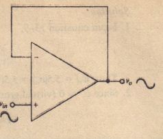
The reader may wonder why it would be desirable or necessary ‘to use an amplifier to multiply a voltage by a number less than I, since this can also be accomplished using a simple voltage divider. The answer is that the amplifier provides power gain to drive a load. Also, the ideal amplifier has zero output impedance, so the output’ voltage is not affected by changes in load impedance. Figure 13-6 shows a special case of the noninverting amplifier, used in applications where power gain and impedance isolation arc of primary concern. Notice that Rf:::: 0 and RI 00, so, by equation 13-15, the closed-loop gain is v)Vj/l = 1 + R/RI 1. This configuration is called a voltage follower because Va has the same magnitude and phase as ViII’ Like a BJT emitter follower, it has large input impedance and small output impedance, and is used as a buffer amplifier between a high-impedance source and a low-impedance load .
In a certain application, a signal source having 60 k!l of source impedance produces a I-V-rms signal. This signal must be amplified to 2.5 V rms and drive a l-kn load. Assuming that the phase of the load voltage is of no concern, design an operationalamplifier circuit for the application.
Solution. Since phase is of no concern and the required voltage gain is greater than I, we can Liseeither an inverting or noninvcrting amplifier. Suppose we decide to use the inverting configuration and arbitrarily choose R, = 250 kn. Then,
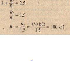
Clearly (he large source impedance is responsible for a reduction in gain, and it is necessary to redesign the amplifier circuit to compensate for this loss. (Do this, as an exercise.) – In view of the fact that the source impedance may not be known prccisc.y or ‘-may change if a replacement source is used, a fur better solution is to design a noninverting amplifier. Since the input impedance of this design is extremely large, the choice of values for R,and R, will not depend on the source impedance, Letting Rf = 150 kfl. we have
The completed design is shown in Figure 13-7. Since we can assume that the amplifier has zero output impedance, we do not need to be concerned with voltage division between the amplifier output and the l-kfl load.


